This article is about my Scanning Electron Microscope (SEM) which I had at home for several years during the time I was doing my graduate studies. I later donated it to Ben Krasnow from California, USA, he is the person who runs the popular science/technology YouTube channel by the name Applied Science.
During the years when I was doing my graduate studies I also worked as a research assistance at the department for material physics. At the time they had an older but still fully functional SEM which was about to be replaced with newer instruments. Due to a lack of space to store the instrument in and also the age of it, they were considering just throwing it away. But the responsible person knew that I was very interested in the technology and apparently thought that I would be suitable person to take care of it.
Hence I was offered to take the microscope, free of charge. This was a microscope which could magnify objects to 100,000x times and had an original retail price of close to $100,000. An offer I definitely could not decline.
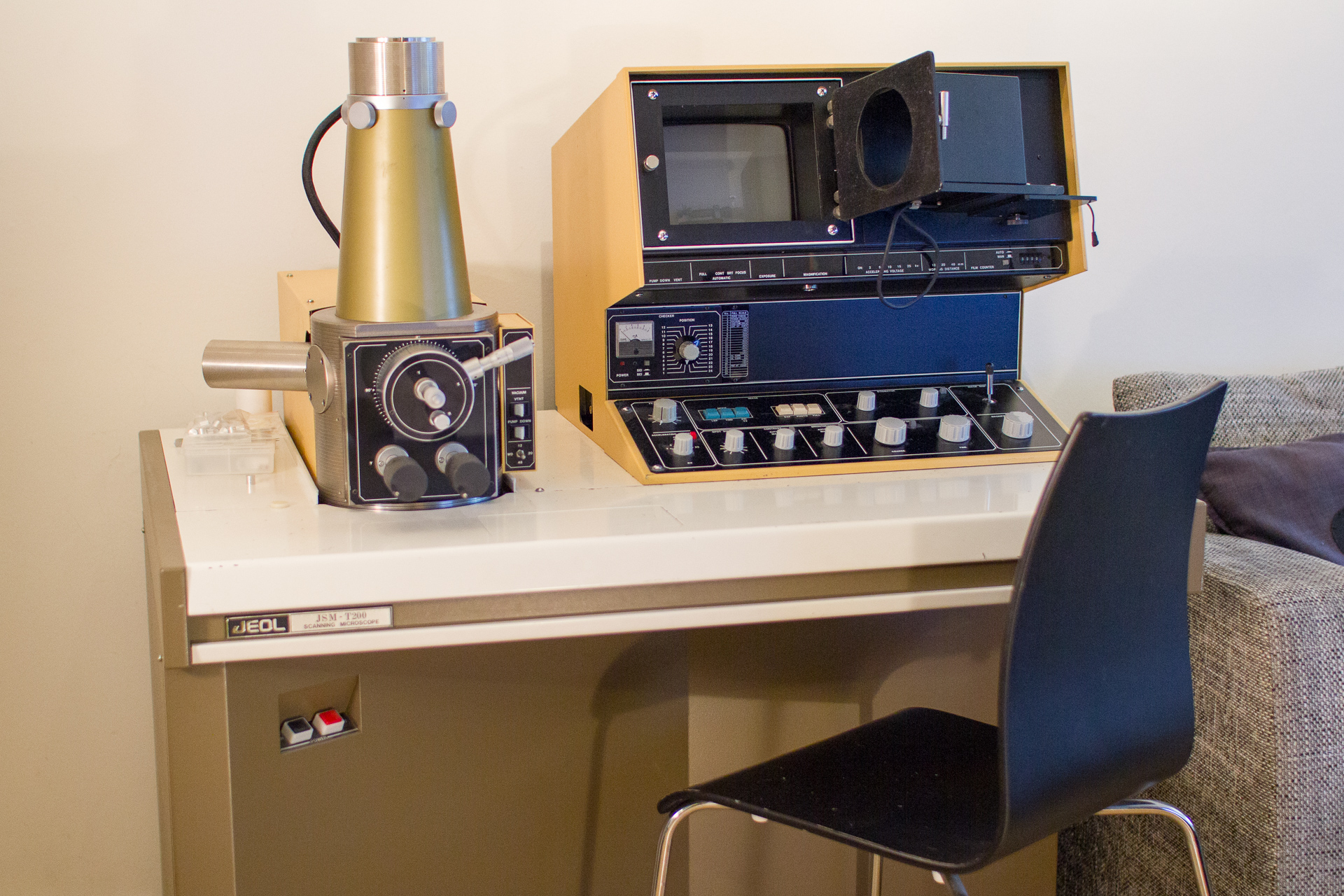
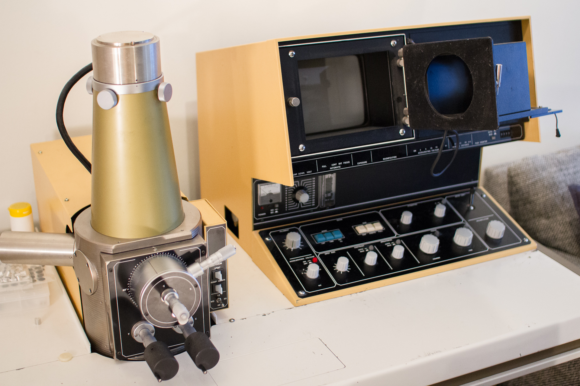
Photographs of the Scanning Electron Microscope, a “JEOL JSM-T200″ as it was standing in my living-room, vacuum chamber and sample stage to the left, control panel and display to the right.
The SEM was a JEOL JSM-T200 which was manufactured in the early 1980’s, it was marketed as a smaller and more user-friendly SEM since it was highly automatized. It had a specified resolution of 10 nm and it came with both secondary and back-scatter electron detectors (SE, BSE). It also had two separate stages, one with 5 axis of movement (X, Y, Z, Tilt, Rotation) and one for extra large samples (ca. 1 dm³). These specifications are comparable to most of the smaller modern SEMs produced today. The reason for this is that the electrons optics are essentially the same in modern microscopes, it is mostly the user interface that has changed towards modern computers with digital sampling instead of analog film.
Having this SEM at home allowed me to analyze a wide variety of samples on my spare time and thus learn about materials or physical phenomena in a hands-on and practical way. Such as high-vacuum systems, electron optics and the electron gun/particle accelerator mechanics, which are rarely thought at universities today.
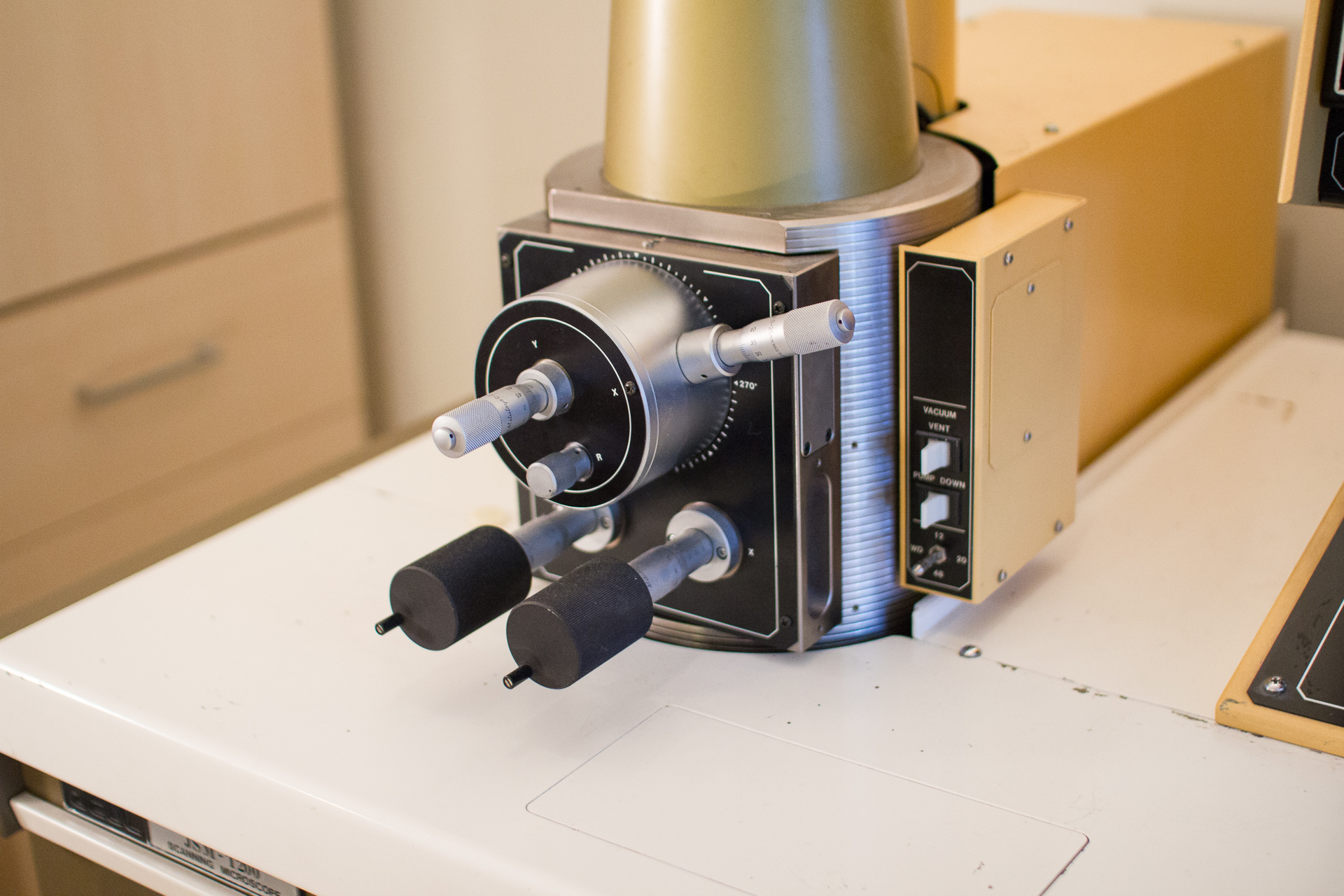
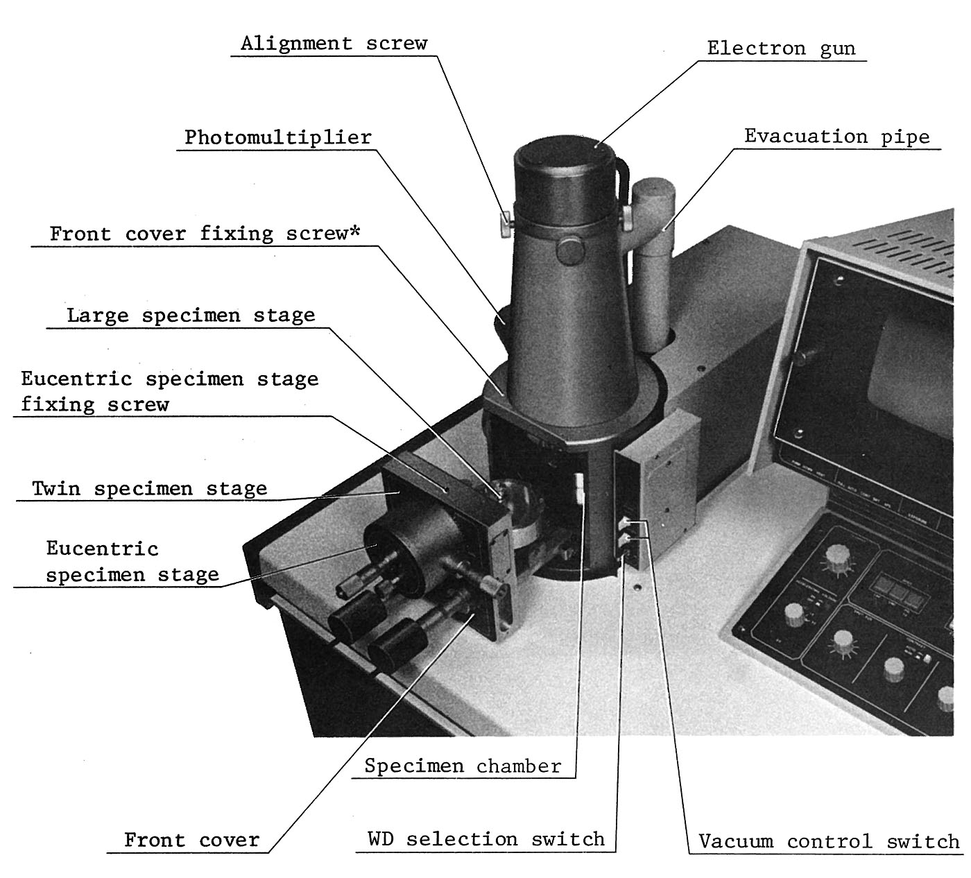
Photograph of the column and sample stage controls (left), scanned description and schematic image from the original JSM-T200 manual (right).
Typically all electron microscopes (SEM and TEM) have their electron gun at the top of the column and high-vacuum is necessary so that the electrons which are accelerated towards the sample does not collide with gas molecules. The JSM-T200 uses on of the most common technique to generate the electrons, a tungsten filament shaped into a sharp tip (V-shape) is heated via electric current so that thermionic emission can occur. This allows electrons to “jump” from the surface of the filament when it is negatively biased towards the positively biased (grounded) sample. The heating is done with just a few volts across the filament, however the biasing voltage from the filament to the sample, is typically on the order of several kV.
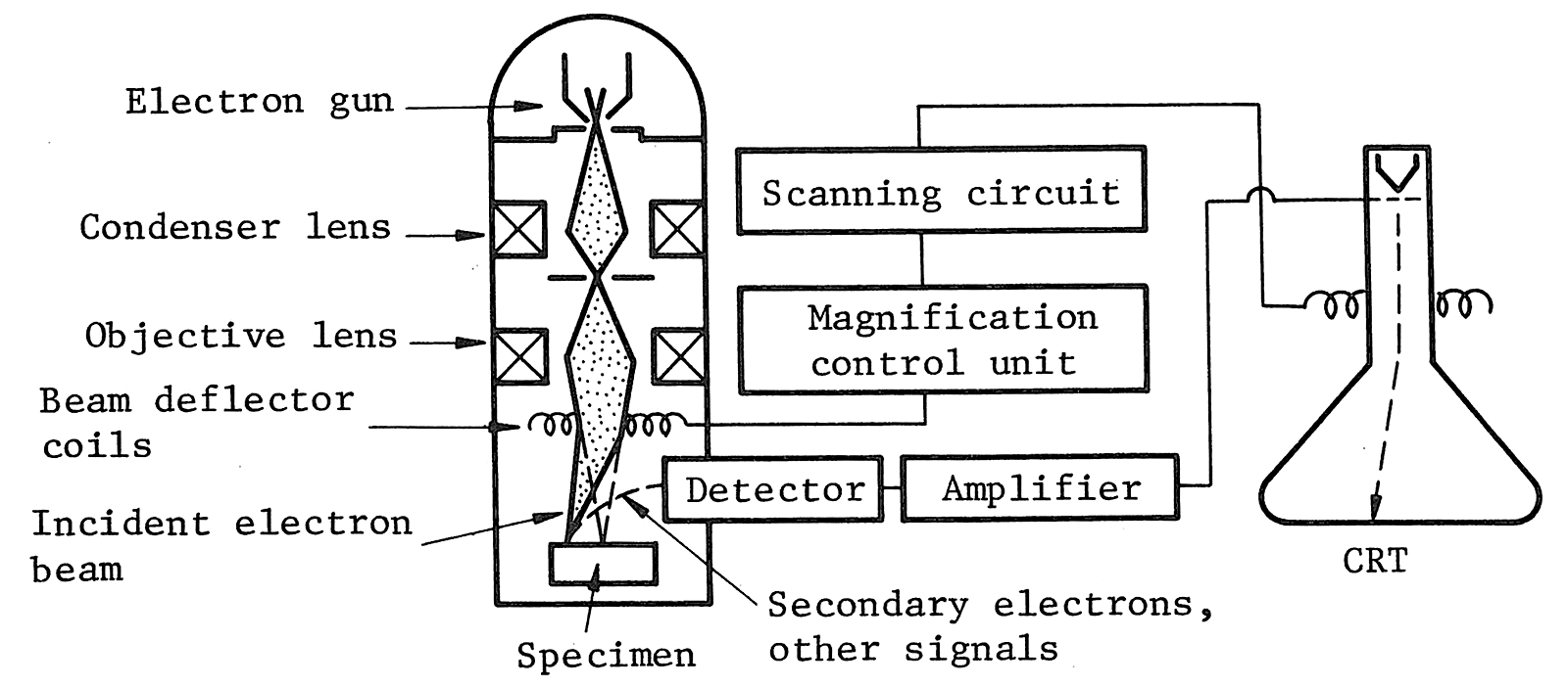 Block diagram showing the working principle of Scanning Electron Microscopes (modern SEMs use computer screen instead of CRTs), image taken from the original manual of the JSM-T200.
The electrons travel from the filament towards the sample and are focused by the means of magnetic lenses (electrostatic lenses also work, but are rarely used in microscopes). The focused beam of electrons are then filtered through apertures so that only a narrow beam of electrons remains. As this narrow beam of primary electrons hit the sample in one particular spot, it “collides” with the electrons in the sample and some of the primary electrons bounce out again (back-scattered electrons), also many of the electrons originally from the sample are also ejected from the surface of the sample (secondary electrons). Some of these electrons hits the electron detector (scintillator and photomultiplier tube) which is mounted close to the sample and are thus measured and counted towards the brightness in that particular spot in the final image. The beam is then “moved” towards the next spot on the sample (next pixel in the image) via the use of deflector coils (or electrostatic plates). Hence an entire image is built up “pixel” per “pixel” as the beam is scanned across the sample.
I demonstrate how the microscope works in greater detail in this YouTube video:
Finally I want to show some of the micrographs I have taken with this SEM, first is a light bulb filament from the very small light bulb which came from a small Maglite® flashlight.
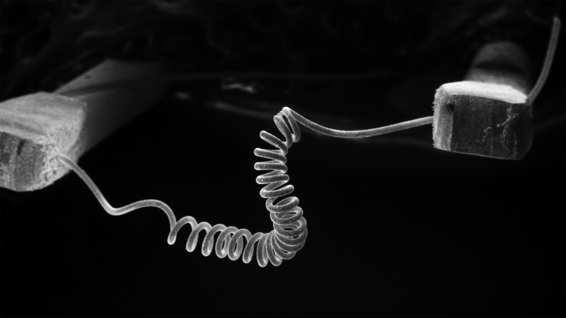
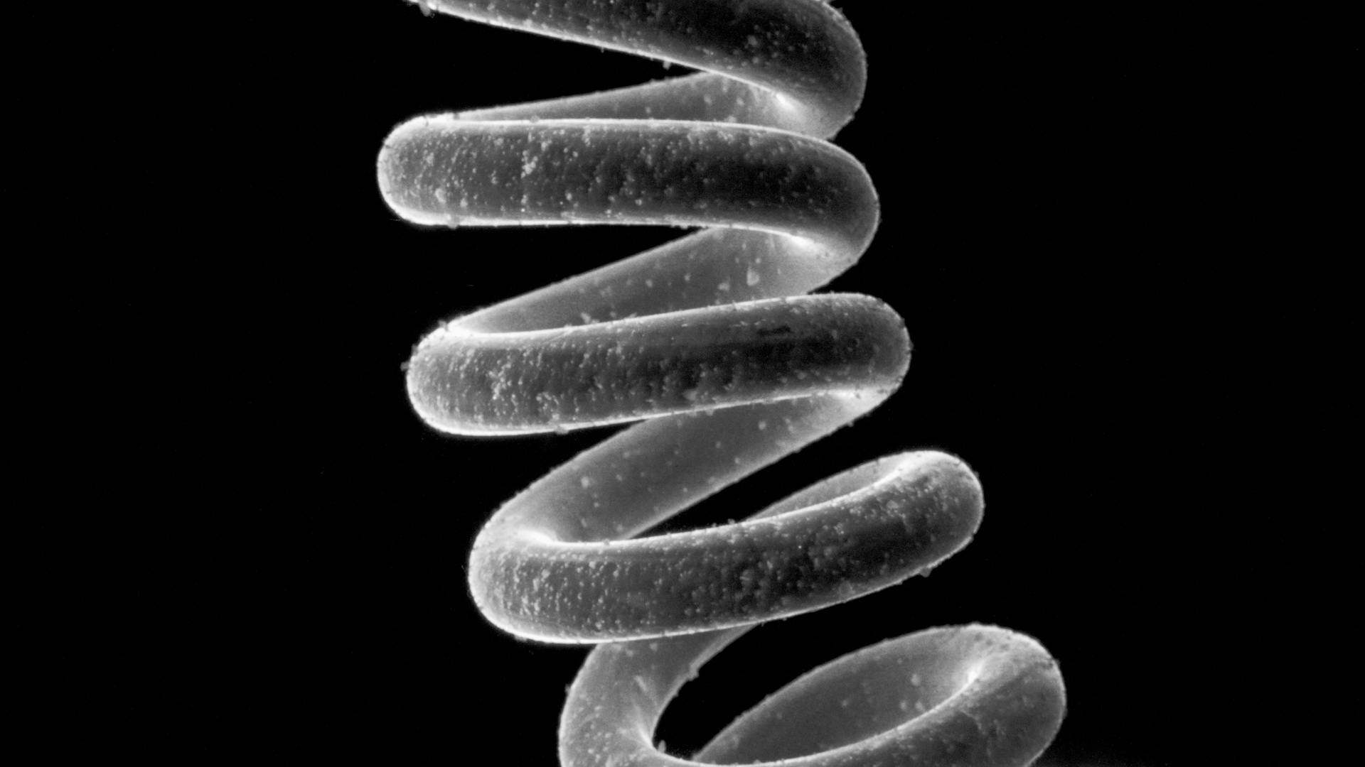
Micrograph of a small light bulb filament, the wire is 20 μm in diameter and the outer diameter of the coil is close to 100 μm (a human hair is about 80 μm).
Another interesting object is an integrated circuit (IC) such as a microprocessor. Unfortunately most modern processors are encapsulated in a composite casing consisting of a cross-linked polymer (often epoxy-based) making it very difficult to extract the semiconductor die. However slightly older microprocessors often had built-in memory which could be erased by the means of UV-light. Hence the package they came in had a quartz window right over the die which I could remove and thus expose the die.


Micrograph of an Intel 8742 microprocessor, the width of the electrical tracks is ca. 5 μm and the height of the font is less than 100 μm.
This is the final photograph of the SEM just before I shipped it to Ben Krasnow at Applied Science in California, USA.
 Final photograph of the microscope as I was packaging it in a wooden crate for its trip to USA.
If anyone is interested, I have scanned the full manual and it is available for download here: JEOL JSM T200 Manual.